
NOTE: This page is being updated.
This page describes the circuit used in the v2.2 HW for the Bob-clock. The v2.1 HW is very similar - the differences will be described in the section named Bob-clock v2.1 hardware. If you want to know about how the circuit for the Bob-clock works, this is the page for you. The v2.0 HW differed in many ways. There is a separate page describing the old circuit (v2.0 HW).
The LED matrix and driving in the v2.2 HW (and v2.1) is basically the same as the v2.0 HW. Since the schematics for the Bob-clock has been cleaned up somewhat in the progress (and we are now using different parts, because we changed all components to thru-hole technology), here is an updated schematic of the LED matrix.
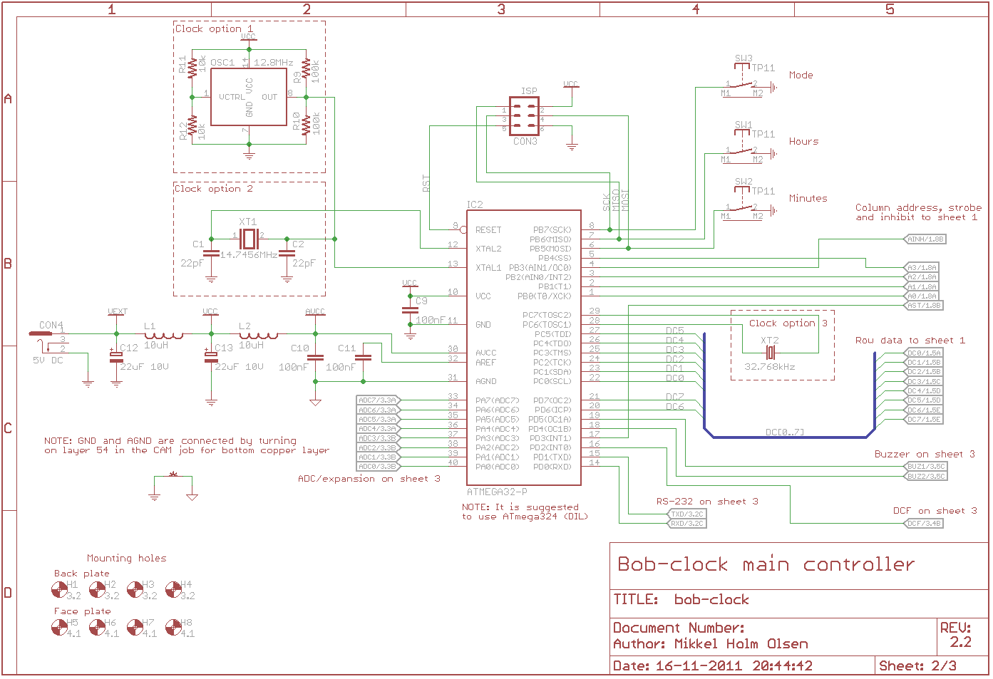
The LEDs are logically arranged into an 8 by 8 matrix, giving 8 × 16 connections (since each LED has one cathode and two anodes). The 8 cathode connections (rows) are connected through current limiting resistors R1-R8 to the N-channel FET drivers T1-T8, which are controlled directly from the microcontroller (signals nets are named DC0-DC7). The low 6 bits are controlled by PC0-PC5, and the remaining two by PD6 and PD7. Of course it would be preferable to use only one port on the MCU, but since we wanted to keep the option of using a 32kHz watch crystal for the time base (clock option 3), we had to liberate PD6 and PD7.
To drive the anodes (columns), there are 16 P-channel FET drivers T9-T24. The power for the LEDs comes from VEXT, which is taken directly from the 5V DC input. Since we now (compared to the v2.0 HW) use the same voltage for driving the LEDs as for the logic, we got rid of the level conversion between the MCU (IC2) and the 4515 demultiplexer (IC3). The outputs from the MUX are inverted, whuch means that all outputs will be logic high, except the one that is selected (which will be low). This is perfect for driving our P-channel FETs, because they conduct when the gate voltage is low. When the INHibit input on the MUX is high, all outputs from the MUX will be high, so no column drivers are enabled (and all LEDs are off).
Perhaps you noticed that the LED drive signals are actually reversed when compared to the MUX outputs (e.g. DG0 is driven by MUX output S15). Because the address lines on the MUX were inverted in the v2.0 HW design, I had re-mapped the outputs, so address 0000 would be the first LED group, 0001 would be the second, and so forth. Unfortunately I had forgotten this when removing the level-shifting and inversion (when designing the v2.1 HW), so the addressing got messed up. Luckily this was easy to fix in the firmware, by simply inverting the 4 address outputs for v2.1 and v2.2 HW. This is now implemented as a table lookup, where the table is defined at compile time, depending on what HW you are compilng for, so the firmware is (compile time) backwards compatible.
Notice the 100kΩ pull-up resistor (R15) on the INHibit pin of the MUX. This was added in HW v2.2. The purpose is to make sure none of the column drivers are on when the circuit is powered, but the MCU is not running, e.g. during programming.
The MUX control signals (A0-A3, AST and AINH) come directly from the MCU. Looking at the main circuit schematics, you can see that A0-A3 are controlled by PB0, PB1, PB2 and PB4. AINH is controlled by PB3, while AST is controlled by PD3. This was different in the v2.1 HW, but by moving AINH to PB3, which can also serve as OC0, we can use the MCUs HW PWM generation to implement a global dimming (e.g. to adjust the overall light level of the clock based on the ambient light sensor).
The firmware implements the LED multiplexing by setting up the address lines A0-A3 and then strobing AST. This means the MUX latches (remembers) the selected address. When the INH input is driven low, the selected output goes low, driving the base of the corresponding FET column driver (T9-T24), thereby enabling the column. In other words we now have a group of 8 LEDs selected, along with the color. We can then output 8 bits in the row-drives, to turn on the desired LEDs in this group. The firmware does this very quickly, so depending on various options (e.g. the selected clock source and the range of dimming) all LEDs are scanned about 100 times per second.
The firmware divides the time equally among the 16 columns, so when an LED is lit, it will still only be on for 1/16th of the time. The LEDs used in the first v1.0 HW were not that bright, and the driver circuit had multiplexers on both rows and columns, so only one LED could be turned on at a time (compared to 8 with the current design). Also, the driver circuit was not quite as powerful, so in that version I switched on only the LEDs needed to display the time (one for the hours, one for the minutes), resulting in a 50% duty cycle. So the new circuit has a draw-back that it can only use 1/16th duty cycle, but this also means that each of the LEDs are individually controllable, so it is actually possible to light every LED. This gives a lot of possibilities for fancy display modes in the firmware.
Of course the LED matrix is not physically positioned in a matrix formation, but rather in a circle (with the last four LEDs being left out). Check out the PCB artwork to see how this was accomplished. The top layer is pcb-top.pdf (40kB PDF) and the bottom layer is in pcb-bot.pdf (49kB PDF).
On the top layer, the LED anodes are connected in groups of 8, each going to one of the P-channel FETs driven by the 4515 outputs. These are actually the columns in the schematics for the LED matrix.
The bottom layer is more complex, with the eight matrix rows being routed as 8 parallel tracks around the circle of the clock. You can see how the connections from the 8 current limiting resistors (R1-R8) are routed to the common cathode (center) pin of the first 8 LEDs. From there the circuit trace continues, running in parallel around the circle, and shifting one position for each LED. After each group (i.e. all 8 row signals are connected to a LED in this group), the 8 parallel tracks all shift back and the same pattern starts over for the next LED group.
The entire PCB design was routed manually, mainly to have complete control over the placement of the tracks (especially the LED matrix). Another reason was that I was going to be making the PCBs with the normal photo-process, and so I would not be able to get it plated through. By doing manual routing I was able to avoid vias.
The Bob-clock has various clock options, which can be selected when compiling the firmware. The 3 clock options are shown on the main schematics. Although the clock options influence several different aspects of the Bob-clock functioning (e.g. the LED multiplexing frequency and baud rate generation if using the serial port), the main thing to consider when selecting clock options is the accuracy of the real-time clock (RTC). The different clock options will be described below.
The most accurate and easiest clock source to use for the Bob-clock is the Voltage Controlled Temperature Compensated Crystal Oscillator or VCTCXO. As the name suggests, this clock base consists of a crystal oscillator, but since the resonance frequency of a quartz crystal is somewhat temperature dependent, a temperature compensation circuit is built into the device.

The particular device used for the Bob-clock also has an input for slightly adjusting the output frequency, by applying a voltage. In the Bob-clock circuit this voltage is formed by the voltage divider R11/R12, which basically just sets the output frequency to the nominal frequency written on the VCTCXO. These VCTCXOs actually also have a little trimmer that you can turn to adjust the frequency, but I am quite pleased with the accuracy, so I would advice against trying to adjust it any further.
The VCTCXO used for the Bob-clock was made by a Japanese company called Nihon Dempa Kogyo Co., Ltd. (NDK). The part number is NKG3001B, and the nominal frequency is 12.8 MHz. I found a box (100pcs) of them on eBay for a very resonable price. They are probably a decade or two old, so perhaps they are not quite as accurate as they used to be, but from my experiments, they still seem much more accurate than a simple crystal.
The 12.8 MHz clock frequency is easy to use for time keeping, because we can simply set the prescaler to 1024, and then further divide by 12.500 to get an accurate 1 Hz timer tick. The frequency is also high enough that LED flickering due to the multiplexing is minimal. Unfortunately the frequency is not the best for generating the standard RS-232 baud rates, but it is still possible to make it work (although the current firmware does not support the UART).
The NKG3001B may be difficult to get your hands on. Perhaps you can find a similar VCTCXO (or just a TCXO). I would think they are also quite pricey unless you can find a surplus, like I did. If you can't find a VCTCXO, you can also get good results with the other clock options, but this will most likely require calibration.
NOTE: The text below this point is not finished yet.
The clock comes from XT1, which is a 14.7456MHz crystal. Unfortunately I did not know much about the load capacitance of the used crystal (nor about the theory of how an incorrect load capacitance affects the generated clock). The result was that the clock would drift a little. Maybe only a couple of minutes per month, but still enough to be noticable, and a bit annoying.
I then thought that I could get more accurate results using a watch crystal connected to the TOSC-inputs (PC6 and PC7). Of course this meant that I had to move to of the row driver outputs to a different port, so writing to the LEDs became a little more complex in the firmware. This should have resulted in more accurate RTC timing, because I now got rid of the load capacitance uncertainty, but unfortunately it turned out that the clock was still drifting. I never really figured out what the reason was (perhaps the internal AVR load capacitance still did not match the 32kHz watch crystal).
I then decided to try tuning the clock in the firmware. This required a clock reference (I used the clock on the television), and a decent amount of patience. What I did was set the clock to the reference (to seconds accuracy), and then wait for about a month. Then I checked the reference clock again, figuring out how many seconds it drifted, and also how many seconds had passed since I set the clock. Dividing these two numbers, I now had the number of seconds that should pass before adding or subtracting a "leap-second". This was implemented in the firmware as a counter that would simply count the number of seconds, and when the set number of seconds had passed either add or subtract one (adding or subtracting was of course based on whether the clock drifted ahead or behind). The nice thing about this approach is that the drift is pretty small to begin with, which means you get very good resolution.
Of course this looked a bit strange after I implemented the clock displaying seconds. All of a sudden the clock would skip one second ahead (OK, I guess nobody would notice, because this happened so rarely, but I knew it was happening occationally, so I came up with a better method). To fix this I implemented sub-seconds for the leap-counter. In other words I would internally keep time in 1/64th of a second, and also use this for the leap-counter. So the counter would expire 64 times as often, but then I would adjust the time by only 1/64th of a second. The leap-counter calibration is in my 2.0 firmware, and will be merged into the 2.1/2.2 branch as soon as I get the time.

Then I finally found a better way to fix the problem, which would not
require calibrating the clock: I bought a bunch of VCTCXOs off of eBay. A
VCTCXO is a Voltage Controlled Temperature Compensated Crystal Oscillator. In
other words this is still based on a quartz crystal, but since we know that
the oscillation frequency of such a crystal varies with changing temperatures,
the VCTCXO measures the temperature and uses this to adjust the frequency
output of the crystal (how this works in detail is beyond the scope of this
article, but the bottom line is that we get much more accuracy out of the
VCTCXO than we would with a crystal). The VCTCXOs I found are 12.8MHz types,
so the firmware was adjusted to use this for the main clock, and also use it
for the RTC. Using a VCTCXO is definitely the easiest option, since it gives
a much more accurate clock, without the need for calibration. But the VCTCXOs
are also a bit expensive, and could be harder to get, so if building a
Bob-clock, you might want (or be forced) to use a regular crystal, and do the
calibration as described above.
Bob-clock v2.1 hardware
There are only minor differences between the v2.1 and v2.2 hardware. These are described in this chapter. Only 3 prototype PCBs were made with the v2.1 design, and one has already been modified to be v2.2 compatible.
The v2.1 HW design did not have a pull-up (R15) on the INHibit pin of the MUX (IC3). This was not critical, but resulted in irratic flashing of the LEDs during programming, because the MUX address inputs were floating.
Cannot use HW PWM for global dimming.
 Electronics
 Nostalgia
 Projects
 Personal
 Links
Links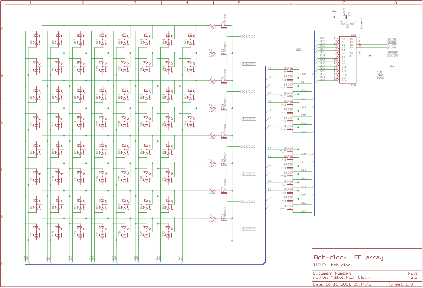